SMPS POWER SUPPLY for ATX COMPUTERS
| Home | Reference | ATX3 pinout | Magnetic Units | SMPS Tutorial |
| Color Codes | Metric Conversion | Computer PSU | Calculators | ATX pinout |
All electronic systems and equipment regardless of their size or function have one thing in common: they all need a power supply unit (PSU) that converts input voltage into a voltage or voltages suitable for their circuits. The most common type of today's PSU is the switch mode power supply (SMPS). There is a wide variety of SMPS topologies and their practical implementations used by PSU manufacturers. However they all use the same basic concepts. This page explains the principals of operation of a switching mode power supply and reviews its main parts and functions. This tutorial can be useful for system integrators, hobbyists, and those who are not necessarily experts in power electronics.
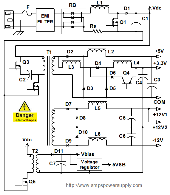 This is a conceptual circuit diagram of the power train of a typical ATX computer power supply unit. This schematic does not show the control circuitry, that's why you see all MOSFET gates and transistor bases are open. For clarity, the parts responsible for miscellaneous auxiliary functions, such as current limit, fan control, and OV protection, which are not essential for learning the basic concepts of the power conversion, are not shown as well. For a complete schematic, see for example this annotated diagram of an ATX power supply.
Note that unlike generators that convert energy stored in various fuels into electricity, PSUs convert electric energy from one form to another. The AC input receptacle in a PC is an IEC 320 type or equivalent. The fuse "F" is followed by an EMI filter. The filter is normally consists of a combination of differential mode and common mode chokes and capacitors. Its main purpose is to reduce the conducted radio frequency noise emitted from the power supply back into the input line to comply with regulatory requirements. Reducing conducted noise also reduces radiated emissions from the input power lines that act as an antenna. The input section usually also includes inrush current limiting and surge protecting components. The EMI filter in most off-line SMPS PSU is followed by a rectifier bridge (RB) and a power factor correction (PFC) stage. This stage was absent from older SMPS, in which the rectifier was followed by a large storage capacitor. Power supply manufacturers began introducing PFC technique beginning late 80's when Europeans introduced EN61000-3-2 norm. This document specifies the maximum amplitude of line-frequency harmonics for various categories of equipment. Our diagram shows a typical PFC stage that consists of a full-wave rectifier and boost converter with a storage capacitor C1. Note that in this scheme the current always flows through two diodes of the rectifier bridge. There are also so-called “bridgeless PFC” which eliminate one diode from the current pass. The storage capacitor is designed to provide energy to the output during short input power interruptions. In practice, there may be several paralleled storage caps. The computer power supplies as well as commercial units normally have to ride through at least one cycle of input sine wave, which is 16 ms in U.S. and 20 ms in Europe. The PFC boost provides DC-link voltage (Vdc) which is higher than the peak of input AC. In modern computer PSU, this voltage is typically 375-400 VDC. If you are trying to troubleshoot a unit and you measure about 160VDC across C1-- it means the boost stage does not work. The output DC-DC stage in any SMPS always contains one or more switching devices that periodically commutate LC networks.
The above diagram shows a so-called forward converter with active reset. Half-bridge is also often used in the PC designs. See examples of schematics based on half-bridge: 250W and 300W.
The main switch Q2 periodically applies voltage Vdc to the primary of power transformer T1. When Q2 is in "on" state, positive voltage appears at the upper terminals of the T2 secondaries. As the result, rectifier diodes D2, D4, D7 and D9 conduct, and the energy from the input source is delivered to the loads. At the same time some energy is also accumulated in the cores of T2 and inductors L2, L4, L5 and L6. When Q2 is in "off" state, the voltages across the secondaries of T2 reverse polarities and rectifier diodes become reverse biased. Since the output inductors still try to maintain the current flow, the polarity of the voltages across them reverse according to Faraday law. As the result, the inductors continue conducting via freewheeling diodes D3, D5, D8, and D10 thus maintaining close current loops through their respective loads. During this time interval the auxiliary switch Q3 provides clamp and active reset of the transformer core. When Q3 turns off, with a proper circuit design Q2 turns "on" at zero voltage, which reduces its switching losses. Such forward converter with active clamp was originally patented by Vicor Corp. As far as I know, this patent expired world wide in 2002. Of course, you should consult your patent attorney for all decisions.
 The control circuit regulates 5V output by using pulse-width modulation (PWM). The 3.3V buss is derived from the same secondary winding as 5V. You can see there is an additional inductor L3 is the 3.3V current pass. This is a magamp inductor. It is used to block a portion of the pulse in order to reduce the regulated voltage to 3.3V. An auxiliary transistor Q4 sets the reset current of magamp inductor L3. This current determines the volt-seconds blocked by L3. The +3.3 VDC error amplifier (not shown on the diagram) often uses remote sensing to compensate for excessive voltage drop in the cable.
Outputs #3 and 4 (+/-12V) in the described power supply are semi-regulated. They are not regulated by an individual closed loop control, but are partially stabilized by the PWM acting on the main 5V buss.
All DC outputs are then brought to standardized harness connectors. Here is a pinout of the main ATX connector. Also see our complete guide to all PSU connectors. Note that modern ATX systems have at least two 12V rails: +12V1 and +12V2. However, in most cases both are coming from the same physical 12V output.
A separate flyback converter consists of power MOSFET Q5, transformer T2, rectifier D11 and filter capacitor C7. It serves two purposes- to provide bias to the control circuitry and to provide 5V standby voltage (5VSB). This voltage must be present whenever AC power is applied to the supply. It powers the circuits that remain operational when the main DC output rails are disabled. See design example of a simple 12V flyback.
If you want to learn the main SMPS topologies, as well as transformer equations and other design information, get my Power supply practical handbook which costs a small fraction of most textbooks.
This is a conceptual circuit diagram of the power train of a typical ATX computer power supply unit. This schematic does not show the control circuitry, that's why you see all MOSFET gates and transistor bases are open. For clarity, the parts responsible for miscellaneous auxiliary functions, such as current limit, fan control, and OV protection, which are not essential for learning the basic concepts of the power conversion, are not shown as well. For a complete schematic, see for example this annotated diagram of an ATX power supply.Note that unlike generators that convert energy stored in various fuels into electricity, PSUs convert electric energy from one form to another. The AC input receptacle in a PC is an IEC 320 type or equivalent. The fuse "F" is followed by an EMI filter. The filter is normally consists of a combination of differential mode and common mode chokes and capacitors. Its main purpose is to reduce the conducted radio frequency noise emitted from the power supply back into the input line to comply with regulatory requirements. Reducing conducted noise also reduces radiated emissions from the input power lines that act as an antenna. The input section usually also includes inrush current limiting and surge protecting components. The EMI filter in most off-line SMPS PSU is followed by a rectifier bridge (RB) and a power factor correction (PFC) stage. This stage was absent from older SMPS, in which the rectifier was followed by a large storage capacitor. Power supply manufacturers began introducing PFC technique beginning late 80's when Europeans introduced EN61000-3-2 norm. This document specifies the maximum amplitude of line-frequency harmonics for various categories of equipment. Our diagram shows a typical PFC stage that consists of a full-wave rectifier and boost converter with a storage capacitor C1. Note that in this scheme the current always flows through two diodes of the rectifier bridge. There are also so-called “bridgeless PFC” which eliminate one diode from the current pass. The storage capacitor is designed to provide energy to the output during short input power interruptions. In practice, there may be several paralleled storage caps. The computer power supplies as well as commercial units normally have to ride through at least one cycle of input sine wave, which is 16 ms in U.S. and 20 ms in Europe. The PFC boost provides DC-link voltage (Vdc) which is higher than the peak of input AC. In modern computer PSU, this voltage is typically 375-400 VDC. If you are trying to troubleshoot a unit and you measure about 160VDC across C1-- it means the boost stage does not work. The output DC-DC stage in any SMPS always contains one or more switching devices that periodically commutate LC networks.
The main switch Q2 periodically applies voltage Vdc to the primary of power transformer T1. When Q2 is in "on" state, positive voltage appears at the upper terminals of the T2 secondaries. As the result, rectifier diodes D2, D4, D7 and D9 conduct, and the energy from the input source is delivered to the loads. At the same time some energy is also accumulated in the cores of T2 and inductors L2, L4, L5 and L6. When Q2 is in "off" state, the voltages across the secondaries of T2 reverse polarities and rectifier diodes become reverse biased. Since the output inductors still try to maintain the current flow, the polarity of the voltages across them reverse according to Faraday law. As the result, the inductors continue conducting via freewheeling diodes D3, D5, D8, and D10 thus maintaining close current loops through their respective loads. During this time interval the auxiliary switch Q3 provides clamp and active reset of the transformer core. When Q3 turns off, with a proper circuit design Q2 turns "on" at zero voltage, which reduces its switching losses. Such forward converter with active clamp was originally patented by Vicor Corp. As far as I know, this patent expired world wide in 2002. Of course, you should consult your patent attorney for all decisions.
The control circuit regulates 5V output by using pulse-width modulation (PWM). The 3.3V buss is derived from the same secondary winding as 5V. You can see there is an additional inductor L3 is the 3.3V current pass. This is a magamp inductor. It is used to block a portion of the pulse in order to reduce the regulated voltage to 3.3V. An auxiliary transistor Q4 sets the reset current of magamp inductor L3. This current determines the volt-seconds blocked by L3. The +3.3 VDC error amplifier (not shown on the diagram) often uses remote sensing to compensate for excessive voltage drop in the cable.Outputs #3 and 4 (+/-12V) in the described power supply are semi-regulated. They are not regulated by an individual closed loop control, but are partially stabilized by the PWM acting on the main 5V buss.
All DC outputs are then brought to standardized harness connectors. Here is a pinout of the main ATX connector. Also see our complete guide to all PSU connectors. Note that modern ATX systems have at least two 12V rails: +12V1 and +12V2. However, in most cases both are coming from the same physical 12V output.
A separate flyback converter consists of power MOSFET Q5, transformer T2, rectifier D11 and filter capacitor C7. It serves two purposes- to provide bias to the control circuitry and to provide 5V standby voltage (5VSB). This voltage must be present whenever AC power is applied to the supply. It powers the circuits that remain operational when the main DC output rails are disabled. See design example of a simple 12V flyback.
If you want to learn the main SMPS topologies, as well as transformer equations and other design information, get my Power supply practical handbook which costs a small fraction of most textbooks.